
| Pinout for:PCI |
Description : PCI pinout
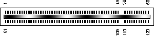
Pinout :
| Pin | Name | Description |
| A1 | TRST | Test Logic Reset |
| A2 | +12V | +12 VDC |
| A3 | TMS | Test Mde Select |
| A4 | TDI | Test Data Input |
| A5 | +5V | +5 VDC |
| A6 | INTA | Interrupt A |
| A7 | INTC | Interrupt C |
| A8 | +5V | +5 VDC |
| A9 | RESV01 | Reserved VDC |
| A10 | +5V | +V I/O (+5 V or +3.3 V) |
| A11 | RESV03 | Reserved VDC |
| A12 | GND03 | Ground or Open (Key) |
| A13 | GND05 | Ground or Open (Key) |
| A14 | RESV05 | Reserved VDC |
| A15 | RESET | Reset |
| A16 | +5V | +V I/O (+5 V or +3.3 V) |
| A17 | GNT | Grant PCI use |
| A18 | GND08 | Ground |
| A19 | RESV06 | Reserved VDC |
| A20 | AD30 | Address/Data 30 |
| A21 | +3.3V01 | +3.3 VDC |
| A22 | AD28 | Address/Data 28 |
| A23 | AD26 | Address/Data 26 |
| A24 | GND10 | Ground |
| A25 | AD24 | Address/Data 24 |
| A26 | IDSEL | Initialization Device Select |
| A27 | +3.3V03 | +3.3 VDC |
| A28 | AD22 | Address/Data 22 |
| A29 | AD20 | Address/Data 20 |
| A30 | GND12 | Ground |
| A31 | AD18 | Address/Data 18 |
| A32 | AD16 | Address/Data 16 |
| A33 | +3.3V05 | +3.3 VDC |
| A34 | FRAME | Address or Data phase |
| A35 | GND14 | Ground |
| A36 | TRDY | Target Ready |
| A37 | GND15 | Ground |
| A38 | STOP | Stop Transfer Cycle |
| A39 | +3.3V07 | +3.3 VDC |
| A40 | SDONE | Snoop Done |
| A41 | SBO | Snoop Backoff |
| A42 | GND17 | Ground |
| A43 | PAR | Parity |
| A44 | AD15 | Address/Data 15 |
| A45 | +3.3V10 | +3.3 VDC |
| A46 | AD13 | Address/Data 13 |
| A47 | AD11 | Address/Data 11 |
| A48 | GND19 | Ground |
| A49 | AD9 | Address/Data 9 |
| A50 | -- | |
| A51 | -- | |
| A52 | C/BE0 | Command, Byte Enable 0 |
| A53 | +3.3V11 | +3.3 VDC |
| A54 | AD6 | Address/Data 6 |
| A55 | AD4 | Address/Data 4 |
| A56 | GND21 | Ground |
| A57 | AD2 | Address/Data 2 |
| A58 | AD0 | Address/Data 0 |
| A59 | +5V | +V I/O (+5 V or +3.3 V) |
| A60 | REQ64 | Request 64 bit ??? |
| A61 | VCC11 | +5 VDC |
| A62 | VCC13 | +5 VDC |
| A63 | GND | Ground |
| A64 | C/BE[7]# | Command, Byte Enable 7 |
| A65 | C/BE[5]# | Command, Byte Enable 5 |
| A66 | +5V | +V I/O (+5 V or +3.3 V) |
| A67 | PAR64 | Parity 64 ??? |
| A68 | AD62 | Address/Data 62 |
| A69 | GND | Ground |
| A70 | AD60 | Address/Data 60 |
| A71 | AD58 | Address/Data 58 |
| A72 | GND | Ground |
| A73 | AD56 | Address/Data 56 |
| A74 | AD54 | Address/Data 54 |
| A75 | +5V | +V I/O (+5 V or +3.3 V) |
| A76 | AD52 | Address/Data 52 |
| A77 | AD50 | Address/Data 50 |
| A78 | GND | Ground |
| A79 | AD48 | Address/Data 48 |
| A80 | AD46 | Address/Data 46 |
| A81 | GND | Ground |
| A82 | AD44 | Address/Data 44 |
| A83 | AD42 | Address/Data 42 |
| A84 | +5V | +V I/O (+5 V or +3.3 V) |
| A85 | AD40 | Address/Data 40 |
| A86 | AD38 | Address/Data 38 |
| A87 | GND | Ground |
| A88 | AD36 | Address/Data 36 |
| A89 | AD34 | Address/Data 34 |
| A90 | GND | Ground |
| A91 | AD32 | Address/Data 32 |
| A92 | RES | Reserved |
| A93 | GND | Ground |
| A94 | RES | Reserved |
| B1 | -12V | -12 VDC |
| B2 | TCK | Test Clock |
| B3 | GND | Ground |
| B4 | TDO | Test Data Output |
| B5 | +5V | +5 VDC |
| B6 | +5V | +5 VDC |
| B7 | INTB | Interrupt B |
| B8 | INTD | Interrupt D |
| B9 | PRSNT1 | Reserved |
| B10 | RES | +V I/O (+5 V or +3.3 V) |
| B11 | PRSNT2 | |
| B12 | GND | Ground or Open (Key) |
| B13 | GND | Ground or Open (Key) |
| B14 | RES | Reserved VDC |
| B15 | GND | Reset |
| B16 | CLK | Clock |
| B17 | GND | Ground |
| B18 | REQ | Request |
| B19 | +5V | +V I/O (+5 V or +3.3 V) |
| B20 | AD31 | Address/Data 31 |
| B21 | AD29 | Address/Data 29 |
| B22 | GND | Ground |
| B23 | AD27 | Address/Data 27 |
| B24 | AD25 | Address/Data 25 |
| B25 | +3.3V | +3.3VDC |
| B26 | C/BE3 | Command, Byte Enable 3 |
| B27 | AD23 | Address/Data 23 |
| B28 | GND | Ground |
| B29 | AD21 | Address/Data 21 |
| B30 | AD19 | Address/Data 19 |
| B31 | +3.3V | +3.3 VDC |
| B32 | AD17 | Address/Data 17 |
| B33 | C/BE2 | Command, Byte Enable 2 |
| B34 | GND13 | Ground |
| B35 | IRDY | Initiator Ready |
| B36 | +3.3V06 | +3.3 VDC |
| B37 | DEVSEL | Device Select |
| B38 | GND16 | Ground |
| B39 | LOCK | Lock bus |
| B40 | PERR | Parity Error |
| B41 | +3.3V08 | +3.3 VDC |
| B42 | SERR | System Error |
| B43 | +3.3V09 | +3.3 VDC |
| B44 | C/BE1 | Command, Byte Enable 1 |
| B45 | AD14 | Address/Data 14 |
| B46 | GND18 | Ground |
| B47 | AD12 | Address/Data 12 |
| B48 | AD10 | Address/Data 10 |
| B49 | GND20 | Ground |
| B50 | OPEN | Ground or Open (Key) |
| B51 | OPEN | Ground or Open (Key) |
| B52 | AD8 | Address/Data 8 |
| B53 | AD7 | Address/Data 7 |
| N54 | +3.3V12 | +3.3 VDC |
| N55 | AD5 | Address/Data 5 |
| N56 | AD3 | Address/Data 3 |
| N57 | GND22 | Ground |
| N58 | AD1 | Address/Data 1 |
| N59 | VCC08 | +5 VDC |
| N60 | ACK64 | Acknowledge 64 bit |
| B61 | VCC10 | +5 VDC |
| B62 | VCC12 | +5 VDC |
| B63 | RES | Reserved |
| B64 | GND | Ground |
| B65 | C/BE[6]# | Command, Byte Enable 6 |
| B66 | C/BE[4]# | Command, Byte Enable 4 |
| B67 | GND | Ground |
| B68 | AD63 | Address/Data 63 |
| B69 | AD61 | Address/Data 61 |
| B70 | +5V | +V I/O (+5 V or +3.3 V) |
| B71 | AD59 | Address/Data 59 |
| B72 | AD57 | Address/Data 57 |
| B73 | GND | Ground |
| B74 | AD55 | Address/Data 55 |
| B75 | AD53 | Address/Data 53 |
| B76 | GND | Ground |
| B77 | AD51 | Address/Data 51 |
| B78 | AD49 | Address/Data 49 |
| B79 | +5V | +V I/O (+5 V or +3.3 V) |
| B80 | AD47 | Address/Data 47 |
| B81 | AD45 | Address/Data 45 |
| B82 | GND | Ground |
| B83 | AD43 | Address/Data 43 |
| B84 | AD41 | Address/Data 41 |
| B85 | GND | Ground |
| B86 | AD39 | Address/Data 39 |
| B87 | AD37 | Address/Data 37 |
| B88 | +5V | +V I/O (+5 V or +3.3 V) |
| B89 | AD35 | Address/Data 35 |
| B90 | AD33 | Address/Data 33 |
| B91 | GND | Ground |
| B92 | RES | Reserved |
| B93 | RES | Reserved |
| B94 | GND | Ground |
Note : PCI pinout